
Nirji Semicon logo

Workforce Strategy

Next-Generation Semiconductor Talent in India: Who's Hiring, Where the Skills Gap Is, and How to Close It

India has moved from semiconductor policy to production. This guide explains who is hiring next-generation semiconductor talent, what institutes are building, where the skills gap really sits, and what it will take to close it.

Short answer

India needs next-generation semiconductor talent across the full value chain: chip design, wafer fabrication, assembly, test and packaging (OSAT/ATMP), equipment service and manufacturing software. Design talent is relatively deep. The sharpest gap is in production-ready technicians, process and equipment engineers, test and packaging specialists, and experienced line leaders. Closing it takes employer-defined roles, hands-on training, competence-based certification and global talent mobility.

Aditya Joshi · · 8 min read

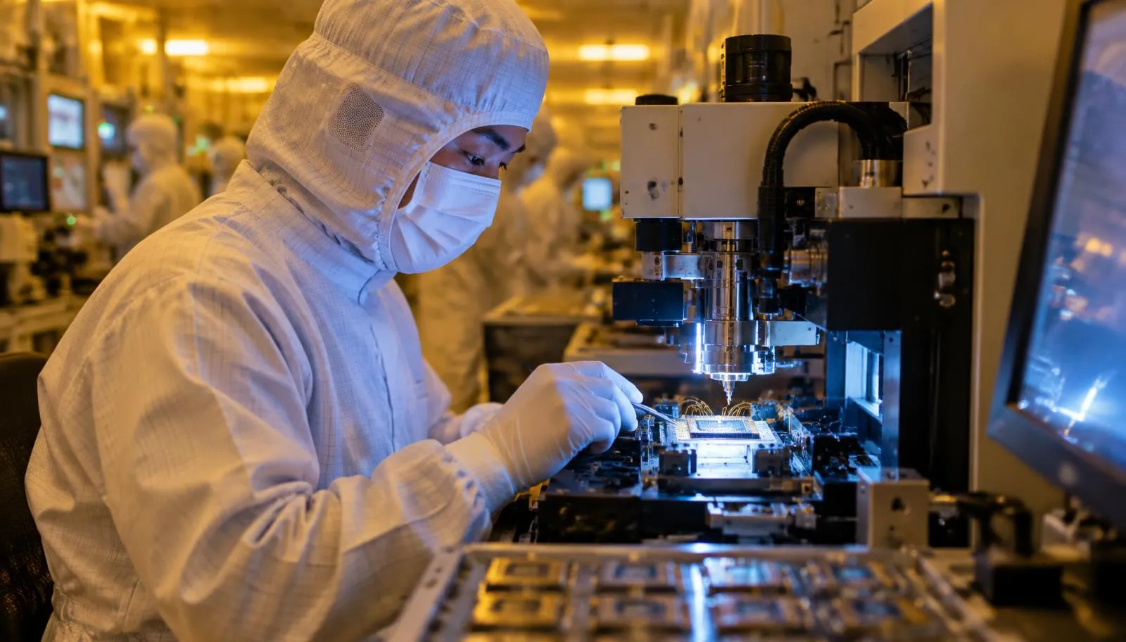
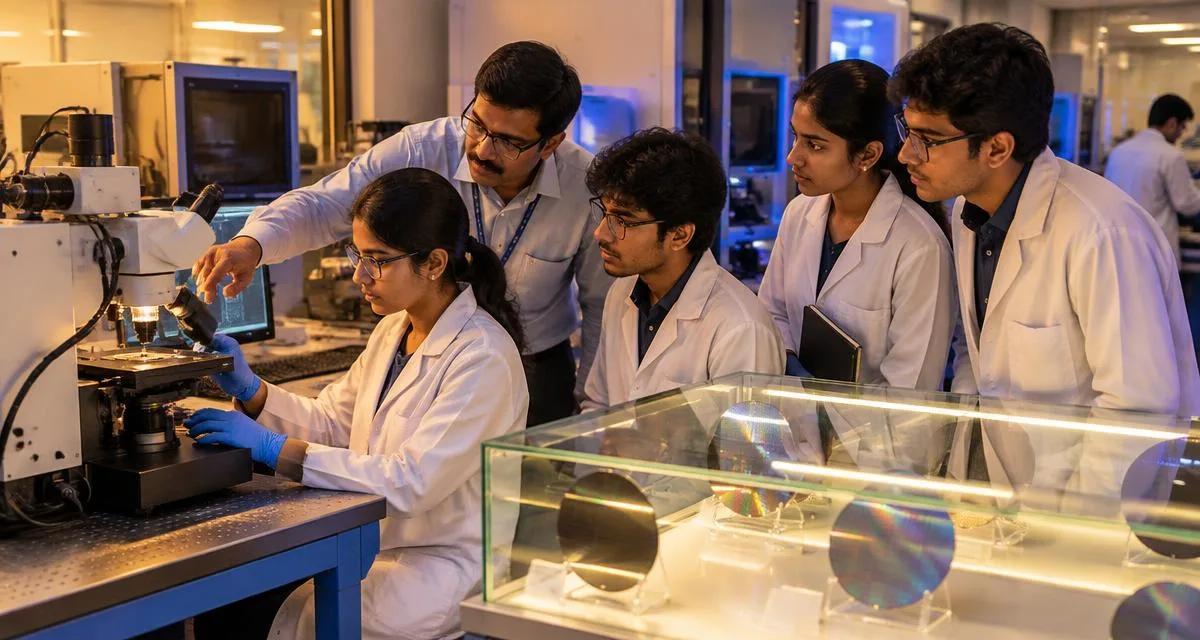
Next-generation semiconductor talent in India across chip design, fab and packaging

India's semiconductor industry has moved from announcements to operations. At SEMICON India 2026 the journey was described as moving "from files to factories". Twelve semiconductor projects were approved under the first phase of the India Semiconductor Mission, several are already in commercial production, and Semicon 2.0, approved in July 2026 with an outlay of Rs 1,27,500 crore, extends the build-out across design, equipment and materials, fabs, advanced packaging and research.

Capital and policy are in place. The question now is people. This guide explains what next-generation semiconductor talent means, who is hiring it in India, what institutes are building, where the gap really sits, and what it will take to close it.

What is next-generation semiconductor talent?

Next-generation (next-gen) semiconductor talent is the workforce that can design, make, package, test and support modern chips at production scale. It is no longer just chip designers. It spans five connected groups:

  • Design talent: architects, RTL designers, verification, physical design, DFT, analog and mixed-signal engineers.
  • Fab talent: process, equipment, yield, metrology and facilities engineers, and cleanroom technicians.
  • OSAT and ATMP talent: assembly, packaging, test, quality and reliability engineers and technicians, including advanced packaging specialists.
  • Equipment and service talent: installation, field service and maintenance engineers who keep tools running.
  • Digital and manufacturing software talent: test programming, automation, MES, data analytics and AI for yield and process control.

What makes this talent next-generation is the combination: strong engineering fundamentals, hands-on tool and process skills, data and programming fluency, and the discipline to work to production standards.

Who is hiring semiconductor talent in India?

Demand now comes from across the semiconductor value chain:

Employer typeWhat they are hiring for
Global chip design centres and fabless companiesRTL design, verification, physical design, DFT, analog/mixed-signal, post-silicon validation, embedded software
OSAT and ATMP plantsAssembly, packaging, test and equipment technicians; process, quality, reliability, yield and maintenance engineers; production supervisors
Wafer fabs and compound semiconductor unitsProcess engineers (lithography, etch, deposition, CMP, implant), equipment engineers, metrology, yield, cleanroom technicians, facilities
Equipment OEMs and suppliersField service, installation and hook-up, applications and customer support engineers
Materials, chemicals and gas suppliersProcess chemistry, quality, logistics, EHS and facilities specialists
Test and qualification service providersTest program, probe card and load board, characterization, reliability and burn-in engineers

Two shifts stand out. Hiring is moving from design-only towards manufacturing, packaging and test, and employers increasingly want people who are productive on day one, not after months of on-the-job training.

What are Indian institutes building?

India's education and skilling ecosystem is responding:

  • Engineering colleges and universities are adding VLSI and semiconductor electives, minors and specialisations, often with industry-standard EDA tool access.
  • Technical and teacher-training institutes have launched focused programmes, such as advanced diplomas in semiconductor packaging and OSAT covering IC package fabrication, ATMP techniques, quality and reliability, and advanced packaging.
  • Skill councils have defined semiconductor qualification frameworks spanning cleanroom practice, processing, vacuum and gas systems, assembly and packaging, and workmanship standards.
  • Polytechnics and ITIs are beginning to prepare technicians for electronics and semiconductor manufacturing.
  • Industry-led academies run by employers and equipment makers train for their own tools and processes.

This is real progress. But building courses is not the same as building a production-ready workforce.

Where is the semiconductor skills gap in India?

The gap is not a shortage of graduates. It sits in five specific places:

  1. Production readiness. Graduates know theory but have rarely worked in a cleanroom, followed ESD discipline, run production equipment, used SPC or worked a shift to SOPs.
  2. Manufacturing over design. India's design talent base is deep; its fab, packaging and test talent base is still thin, and that is where new plants are hiring.
  3. Experienced mid-level and senior talent. New plants need people who have already started up and stabilised lines. In India that pool is small and contested.
  4. Equipment access and trainers. Hands-on skills need real tools or simulators and trainers with industry experience, both scarce.
  5. No common standard for "ready". Certificates usually prove attendance, not ability, so employers re-train and re-test new hires themselves.

The result: capable candidates miss semiconductor careers, while plants carry the cost of training during the ramp, when yield and uptime matter most.

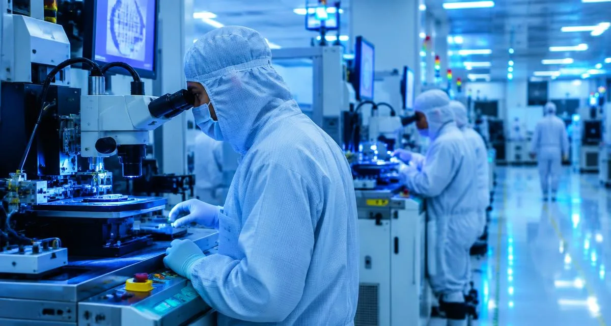
What needs to be done to build India's next-generation semiconductor workforce?

Closing the gap needs coordinated action across employers, institutions and states:

  1. Define roles at competency level. Specify what each role must do, on which equipment, at what proficiency, so training targets real jobs.
  2. Train hands-on, close to production. Combine a shared semiconductor foundation with role-specific and employer-specific modules on real tools or simulators.
  3. Certify demonstrated competence. Assess knowledge, practical ability, safety and quality discipline independently, not just attendance.
  4. Mobilise experienced talent for start-ups. Bring seasoned professionals to India to start lines and transfer know-how to local teams.
  5. Build faculty and trainer capacity. Develop trainers who combine teaching skill with plant experience.
  6. Track outcomes. Measure deployment, time-to-productivity and retention, and feed the results back into programmes.
  7. Build talent where plants are coming. Align state skilling with the industry each state wants to attract.

How is Nirji Semicon building next-generation semiconductor talent?

Nirji Semicon is a semiconductor workforce infrastructure company. We sit between industry demand and talent supply, and build the workforce through three engines:

  • Mobilise. We bring experienced semiconductor professionals from global hubs to India to start and stabilise lines, and to coach local teams on the floor.
  • Manufacture. We build India's own workforce at scale through client-defined workforce programmes, delivered with qualified universities, colleges, polytechnics, ITIs and training partners. Candidates are assessed for Nirji Ready certification, which certifies demonstrated readiness for a defined role and level, not course completion.
  • Deploy. Certified talent joins employers through direct hire or a managed workforce, with performance checked at 30 and 90 days.

The system behind it:

  • Nirji Workforce Architecture: role-by-role competency definitions from technician to engineer.
  • Nirji Academy-in-a-Box: a deployable academy that can run inside an institution, industrial park or employer site.
  • Nirji Talent Cloud: verified competency profiles instead of unverified CVs.

We start where plants are live and roles repeat, in OSAT and ATMP, and extend across fabs, equipment service and design.

Skills in demand across the semiconductor value chain

SegmentCore skills employers look for
Chip designRTL design, Verilog, SystemVerilog, UVM verification, STA, physical design, DFT, analog and mixed-signal design, low-power design
Wafer fabPhotolithography, etch, CVD/PVD/ALD, CMP, ion implantation, metrology, yield engineering, SPC, cleanroom protocol
OSAT and packagingDicing, die attach, wire bonding, flip-chip, molding, wafer-level and 2.5D/3D packaging, reliability, failure analysis
TestATE test programming, wafer sort, probe card and load board, characterization, burn-in
Equipment and servicePreventive maintenance, vacuum and RF systems, wafer handling robotics, PLC, field service
Programming and dataPython, Tcl, Perl, C/C++, embedded C, Linux, MES, SECS/GEM, yield analytics, machine learning

Build next-generation semiconductor talent with Nirji Semicon

You define the workforce. We build it.

Frequently asked questions

What is next-generation semiconductor talent?

It is the workforce that can design, manufacture, package, test and support modern chips at production scale. It spans chip design, wafer fab, OSAT and packaging, equipment service and manufacturing software, and combines engineering fundamentals with hands-on tool skills and data fluency.

Which semiconductor jobs are in demand in India?

Demand covers RTL design and verification, physical design and DFT engineers; process, equipment, yield and metrology engineers in fabs; assembly, packaging and test technicians and engineers in OSAT and ATMP plants; field service engineers for equipment makers; and test programming and automation specialists.

Where is India's semiconductor skills gap?

The gap is in production readiness, manufacturing and packaging skills rather than design, experienced line leaders, equipment access and trainers, and a common standard that certifies demonstrated competence instead of attendance.

How can engineering graduates get into the semiconductor industry in India?

Build strong fundamentals in electronics or a related discipline, gain hands-on exposure to cleanroom practice, equipment, test or design tools, learn programming such as Python or Tcl, and pursue competence-based certification. Joining a talent registry such as the Nirji Talent Cloud connects you with employers.

How does Nirji Semicon help companies hire semiconductor talent?

Nirji Semicon mobilises experienced global talent, builds India's own workforce through client-defined programmes certified to the Nirji Ready standard, and deploys certified talent with performance tracked at 30 and 90 days. Engagements start with a workforce diagnostic.

What is the difference between OSAT and ATMP?

Both describe the back-end stage of semiconductor manufacturing, where finished wafers become packaged, tested chips. OSAT means Outsourced Semiconductor Assembly and Test; ATMP means Assembly, Test, Marking and Packaging. The terms are often used interchangeably in India.

Skills and topics

Share
Aditya Joshi

Aditya Joshi

Co-Founder & CEO

25+ years across semiconductors, technology, workforce solutions and operations. Global operations leadership at Applied Materials including India and China delivery; leadership roles at ManpowerGroup and Capgemini; former CEO of OpalForce. Staffing Industry Analysts 2022 Industry Game Changer and ManpowerGroup Global Power Award 2019.

LinkedIn

Related Insights

Get new Insights by email

Occasional notes on India's semiconductor workforce. No spam; unsubscribe any time.

I am a...

Employer

Tell us your roles, volumes and ramp dates. We map the workforce your line needs and show how to mobilise, manufacture and deploy it.

Request a Workforce Diagnostic

Equipment OEM

Tell us your install base, tools and service commitments. We'll plan the service workforce to support them.

Request a Field Service Workforce Plan

State government

Tell us the semiconductor industry you want to attract. We will help build the workforce ecosystem to support it.

Start a State Workforce Diagnostic

Institution

Bring semiconductor pathways to your campus. Tell us about your institution and we will set up a capability conversation.

Become a Delivery Partner

Candidate

Build your semiconductor career. Create your profile and get matched to roles and workforce programmes.

Join the Talent Cloud

Global professional

Bring your semiconductor experience to India. Register and we will match you to opportunities.

Register for India opportunities